
Intermetallics and Why They Matter
Welcome back to WISDOM WEDNESDAY! In this post we’ll take a closer look at the roles that different metals play in the production of PCB assemblies. Then we’ll touch on the combinations of metals known as intermetallics that provide for the transport of electrical current across the different interfaces present on PCBAs. Wisdom Wednesday is brought to you by Micron Corporation that manufactures precision electronics at a Micron level.
Different Elements
Many different elements are used in electronics manufacturing. Indulge a bit of chemistry to set the scene. The known elements are collected in a block diagram labelled the Periodic Table of Elements. There are five types of metal groupings in the table: Alkali Metals, Alkaline Earth Metals, Transition Metals, Post Transition Metals, and Metalloids (which are considered partly metallic). We are focusing on three highly conductive Transition Metals; Copper, Silver, and Gold whose elemental abbreviations are Cu, Ag, and Au, respectively. And two Post Transition Metals, Tin (Sn) and Lead (Pb) which are widely used in solder alloys. Tin-lead solder remains available for some high-reliability applications; AIM offers both leaded and lead-free materials for military and aerospace customers.
Those three highly conductive metals (Cu, Ag, and Au) and the other two (Pb and Sn) make up a significant portion of metals used in PCBAs, though there certainly are others. Just a bit more chemistry before we shift gears to how these metals are utilized in electronics. The reason Cu, Ag, and Au are so highly conductive is that all three have one outer (or valence) electron in what are known as their “outer electron shells.” Okay, enough chemistry.
Where are Metals Used
Where are these elemental metals used? Copper is by far the most used as measured by mass (weight). It is used in layered planes, traces, pads, vias, and through holes of PCBs. In fact, there is a measure known as Copper Weight used to describe the thickness of Cu used in a PCB by specifying the mass of it over a given area. It’s also used in the terminations of component leads. Most silver (by weight) is present in the solder (often SAC305) and to a smaller amount with the surface finish known as Immersion Silver. Gold is also used in surface finishes such as Electroless Nickel Immersion Gold (ENIG) and Electrolytic Gold. Tin is also used as a surface finish in relatively small amounts. Tin and lead appear in lead solder, and tin appears in many other solders (such as SAC305).
Intermetallics In Solder Joints
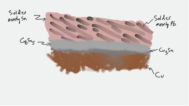
We’ve summarized this information for the purpose of getting to a deeper (or perhaps better stated as inner) subject that is intermetallics. It is hard to overstate the importance of the presence of these intermetallics. Without them there are no viable electrical connections using the metals discussed. They form during the soldering process (whether SMT or through-hole). For the purpose of this discussion we will focus on SnPb solder on a copper pad. Other solders are in broader use these days but the Tin-Lead system on top of a copper PCB pad is the best known and perhaps the most studied. The intermetallics that appear in that system are represented in grey in the drawing below. They are Cu3Sn which grows at the copper interface (reddish at bottom) and Cu6Sn5 which forms at the mostly Tin interface (pink at top). These are crystalline structures that pass current from the copper pad to the component that “sits” in the solder. The drawing in Figure 1 does not show the component leads (or the component) it is a representation of SnPb solder sitting atop a copper pad that has been reflowed to form the intermetallics. The pink with dark streak-like regions at the solder top represent the different phases that are present in the solder. The pink is rich in Sn and the darker streaks are richer in Pb. The whole structure forms a “sandwich” of multiple crystalline layers.
Figure 1. Intermetallic Layers
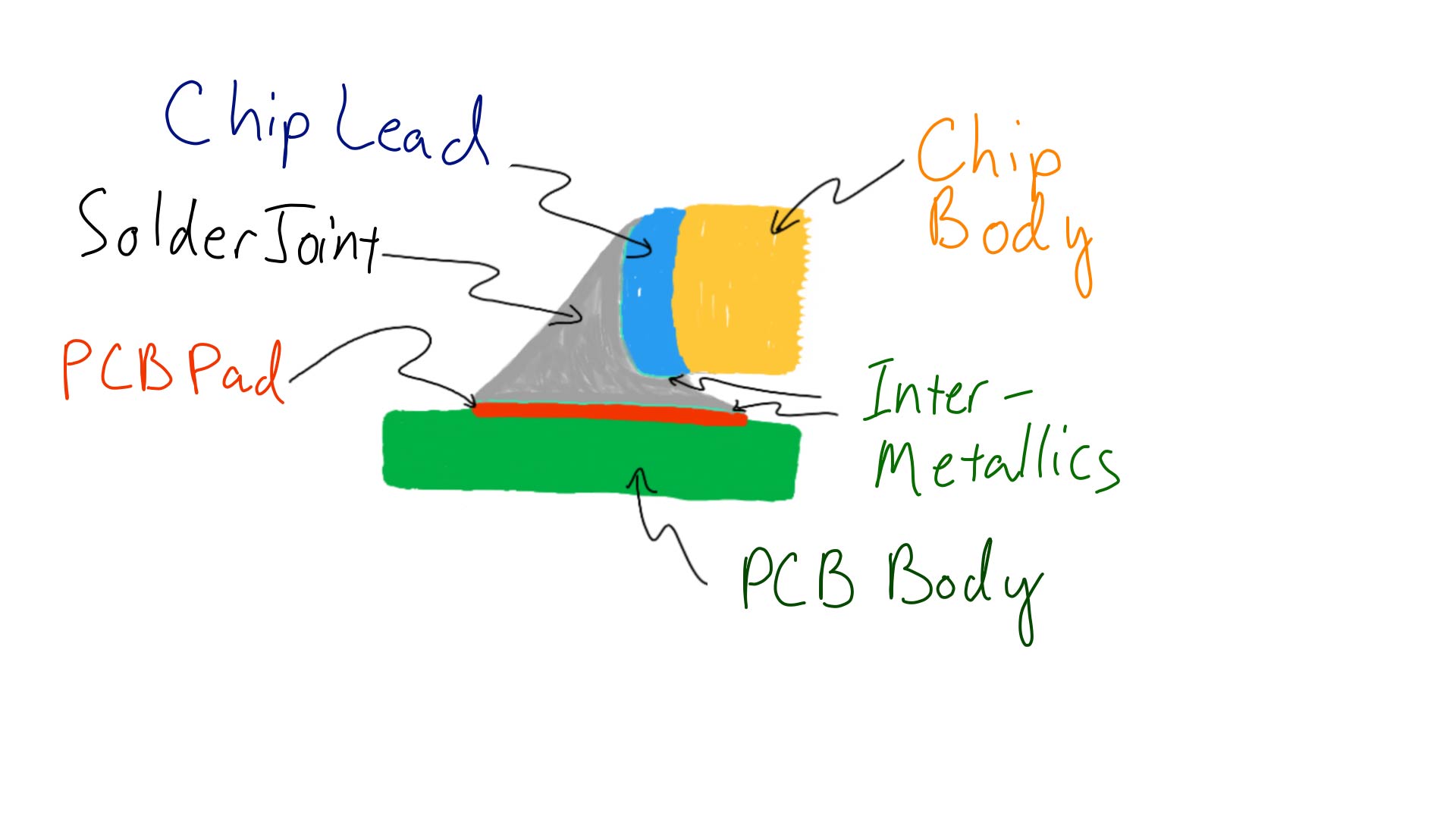
The second drawing gives more information about where the intermetallics are present when a chip resistor (or capacitor) is soldered to a PCB with a copper pad. It shows the chip body in yellow, the chip lead in blue, the solder joint in grey, the PCB copper pad in red, and the PCB in dark green. The intermetallics described in the previous drawing are present in light green at the interfaces between the copper pad and solder, and the chip lead and solder. This morphology allows current to pass from the pad to the chip and from the chip to the pad.
Figure 2. Chip on PCB with Intermetallics
That brings us to the end of this post of Wisdom Wednesday. We look forward to sharing with you again next week. And you can always share information with us at MICRON CORPORATION by contacting info@microncorp.com.
Learn more about the materials behind these joints in Types of Solder Delivery Material and Solder Composition.